
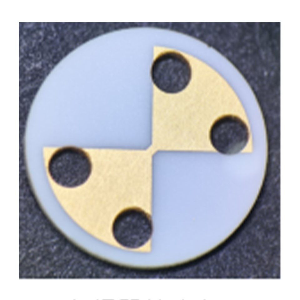


Thin Film Circuit Technology
Description
Technical Parameters
Product introduction
Thin film circuit technology refers to the formation of electronic components using photolithography after the substrate is vacuum deposited into a thin film. This technology has become the preferred approach for making microstrip circuits due to its broad range of component parameters, high accuracy, good batch consistency, high reliability, and good temperature-frequency characteristics. It is mainly applied in medical electronics, high-speed computers, weapons and equipment, aerospace and other fields.


Research Direction
The future of thin film circuit products lies in the direction of smaller line size structures, higher graphic quality and accuracy, improved reliability, reduced volume, and higher application frequency bands.
Technological Process
Punching → Sputtering → Film Layer Thickening→ Photoetching → Scratching → Testing
Product test
1,Test Items: Appearance
Test Tools: Stereomicroscope
Test Methods: GJB548B Method 2032
Technical Index: 80% of the graphic parts are complete, and there is no visible metal residue in non-graphic areas
2,Test Items :Overall Dimension
Test Tools : Vernier Caliper, Electronic Micrometer,Image Measuring Instrument
Test Methods:GJB548B,Method 2016
Technical Index:
| Processing | Normal | High Precision |
| Methods | Precision Error | Error |
| Grindstone | ≤ ± 50 µm | ≤ ± 25 µm |
| Laser | ≤ ± 100 µm | ≤ ± 50 µm |
3,Test Items: Lithographic Metal Graphics
Test Tools :Image Measuring Instrument ,Metallographic Microscope
Test Methods:GJB548B,Method 2016
Technical Index:
| Item | Error |
| Front and Back Engraving | ≤ ±25 µm |
| Same Side Engraving | ≤ ±25 µm |
| Line Size | ±5 µm |
4,Test Items: Membrane Adhesion
Test Tools:3M610 Adhesive Tape
Test Methods:ASTM B571-97 Tape Testing Method
Technical Index :Under a 40X microscope, there is no peeling phenomenon observed on the membrane layer in any form
5,Test Items:High Temperature Resistance of the Membrane Layer
Test Tools:Hot Stage
Test Methods :Keep at 400 ℃ for 10 Minutes
Technical Index: Under a 40X microscope, there is no discoloration, peeling, blistering, or peeling of the membrane layer in any form
6,Other Technical Indexes
| Item | Technical Index |
|
Through Hole |
Substrate Thickness×0.8 |
|
The Minimum Distance from the Guide Band to the Edge of the Ceramic |
0.050 mm |
| Lithographic Minimum Line Width | 0.015mm |
| Resistance | ±10% |
Hot Tags: thin film circuit technology, China thin film circuit technology manufacturers, suppliers, factory, electronic materials and microcircuits, Low Temperature Co fired Ceramic, Thin Film Circuit Technology
Previous
Low Temperature Co-fired CeramicNext
No InformationSend Inquiry


